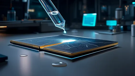
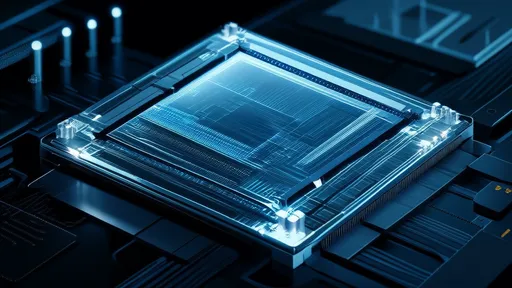
The pursuit of higher bandwidth and lower latency in data centers has driven the rapid evolution of optical communication technologies. Among these advancements, the co-packaging of optics and electronics (CPO) has emerged as a critical solution to overcome the limitations of traditional pluggable transceivers. At the heart of CPO implementation lies the challenge of achieving precise alignment between optical components and integrated circuits, where even micron-level misalignment can lead to significant signal degradation. This article explores the intricacies of photoelectric co-packaging alignment accuracy and its pivotal role in next-generation communication systems.
The Physics Behind Alignment Tolerance
Optical coupling efficiency between silicon photonics chips and optical fibers follows an inverse exponential relationship with misalignment. Experimental data from recent studies shows that lateral displacement beyond 1.5 microns typically results in over 50% power loss for single-mode fiber connections. This sensitivity stems from the fundamental mode field diameter of optical waveguides, which typically ranges between 8-10 microns for standard silicon photonics implementations. The vertical alignment tolerance proves even more stringent, with Z-axis displacements causing rapid deterioration of coupling efficiency due to the Gaussian beam propagation characteristics.
Thermal considerations compound these challenges. The coefficient of thermal expansion mismatch between silicon (2.6 ppm/°C) and common packaging substrates like organic laminates (12-16 ppm/°C) can induce several microns of displacement across typical chip sizes during operational temperature cycling. Advanced packaging solutions must therefore incorporate both passive alignment techniques during assembly and active alignment maintenance mechanisms during operation.
Current Industry Approaches to Precision Alignment
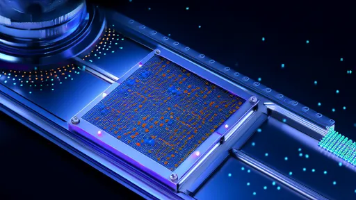
Leading semiconductor manufacturers have developed several competing methodologies to address the alignment challenge. Some opt for active alignment systems using robotic micropositioners with vision feedback, achieving sub-micron accuracy through real-time monitoring of optical power throughput. Others prefer passive alignment techniques relying on high-precision mechanical stops etched directly into the silicon photonics die, leveraging the lithographic accuracy of modern semiconductor processes.
An emerging hybrid approach combines initial passive coarse alignment with subsequent active fine-tuning. This method often incorporates novel fiducial markers detectable by both optical imaging systems and capacitive sensors, enabling multi-modal alignment verification. The most advanced implementations now achieve consistent alignment accuracy below ±0.3 microns in production environments, with laboratory demonstrations pushing below ±0.1 microns using interferometric techniques.
Metrology Challenges in Alignment Verification
Validating alignment accuracy presents its own set of technical hurdles. Traditional optical inspection methods struggle with the three-dimensional nature of photonic coupling, where optimal alignment in one plane doesn't guarantee performance in another. Scanning electron microscopy provides superior resolution but requires destructive sample preparation. X-ray tomography offers non-destructive internal inspection but lacks the resolution for sub-micron features.
Industry leaders are increasingly turning to indirect measurement techniques. These include monitoring the photocurrent generated in integrated germanium photodetectors during alignment procedures or analyzing back-reflection patterns using integrated optical power monitors. Such methods provide real-time feedback without requiring external probing equipment, enabling closed-loop control systems that maintain alignment throughout the device lifecycle.
Materials Innovation for Stable Alignment
The packaging materials themselves play a crucial role in maintaining long-term alignment stability. Conventional epoxy adhesives, while convenient, exhibit creep under sustained mechanical stress and moisture absorption that can gradually degrade alignment. Alternative solutions under development include:
Glass solder materials with precisely matched thermal expansion coefficients, enabling hermetic seals that maintain alignment across temperature cycles. Nano-particle reinforced composites that combine the placement accuracy of polymers with the dimensional stability of ceramics. Direct metal bonding techniques using ultra-thin gold or copper interlayers that provide both electrical connectivity and mechanical fixation.
These material advancements are particularly critical for co-packaged optics destined for harsh environments such as automotive or aerospace applications, where temperature extremes and mechanical vibration pose additional challenges to alignment maintenance.
The Road to High-Volume Manufacturing
While laboratory prototypes have demonstrated the feasibility of precise photoelectric co-packaging, translating these results to high-volume production remains challenging. The semiconductor industry's transition from wafer-level packaging to panel-level processing introduces new alignment considerations, as larger substrate sizes magnify the impact of any process non-uniformities.
Equipment manufacturers are responding with multi-stage alignment systems that combine global fiducial tracking with local pattern recognition. These systems leverage machine learning algorithms to compensate for material distortions that vary across the processing panel. Early production data suggests such approaches can maintain alignment tolerances within ±0.5 microns at throughputs exceeding 1,000 units per hour - a crucial milestone for economic viability.
The ultimate goal remains the development of self-aligning optical interfaces that achieve sufficient precision through designed-in mechanical features alone, eliminating the need for active alignment altogether. Recent demonstrations of silicon photonics chips with integrated alignment funnels and self-centering fiber receptacles show promise in this direction, potentially revolutionizing the economics of co-packaged optics deployment.
Future Directions and Industry Implications
As data rates continue climbing toward 1.6T and beyond, alignment tolerances will become even more stringent. The industry anticipates needing sub-100nm alignment accuracy for next-generation photonic interconnects, approaching the precision levels currently seen in semiconductor lithography. This trajectory suggests increasing convergence between semiconductor manufacturing and photonic packaging technologies.
Standardization efforts led by industry consortia are beginning to address alignment specifications and test methodologies. These developments will prove critical for establishing multi-vendor ecosystems and ensuring interoperability between components from different suppliers. The coming years will likely see photonic alignment accuracy emerge as a key differentiator in data center component markets, driving further innovation in this crucial aspect of photonic integration.

By /Aug 7, 2025

By /Aug 7, 2025
By /Aug 7, 2025
By /Aug 7, 2025
By /Aug 7, 2025

By /Aug 7, 2025
By /Aug 7, 2025

By /Aug 7, 2025
By /Aug 7, 2025
By /Aug 7, 2025
By /Aug 7, 2025

By /Aug 7, 2025
By /Aug 7, 2025
By /Aug 7, 2025
By /Aug 7, 2025

By /Aug 7, 2025

By /Aug 7, 2025
By /Aug 7, 2025

By /Aug 7, 2025
By /Aug 7, 2025